
| Home | People | Publications | Research | Resources |
The Prototype DOT Imager: CW1
CW1 was conceived as an inexpensive and portable continuous-wave DOT system. It was constructed on a shoestring budget, using the technology available and affordable at the time. CW1 contains 18 laser diode sources (9 at 780nm and 9 at 830nm) and 16 silicon detectors, and can acquire 288 independent measurements in less than 4 seconds. These data can then be processed using a variety of imaging algorithms.
Designing the CW1 DOT system
Our goal was to develop a prototype portable diffuse imager which can be used as a research tool for both characterizing tissue optical properties and guiding us toward future hardware and software design improvements. For simplicity, we decided on a magnitude-only system. Our optical sources were low-power commercially available laser diodes. Although more powerful light-emitting diodes were available, coupling that light into the various core sizes of both plastic and glass fiber would have been very difficult and far less optically efficient. Also, the spectral bandwidth of an LED is far broader than that of a laser diode – wide enough to affect the accuracy of the blood volume and oxygenation calculations. Our detector options ranged from multi-anode PMTs to discrete commercial-grade photodiodes with external preamplifiers. We compromised by choosing a monolithic photodiode/preamplifier IC housed in a clear 8-pin DIP package (OPT209 from Burr-Brown, Tucson, AZ). This offered both the convenience and low-cost of a solid-state detector, combined with the electrical and optical isolation of an integrated preamplifier. Although the parasitic capacitances of the monolithic preamp were about twice that of a well-designed discrete circuit, the simplicity and the relaxed electrical shielding requirements for the monolithic preamp swayed our decision.
We wanted the prototype system to provide a useable (i.e. linear) dynamic range of at least 80dB. Dynamic range and linearity are closely paired, since each must be defined with reference to the other. For example, a statement of a given dynamic range value is, in itself, meaningless unless the criteria for determining the limits of that range are expressly stated. In our case, our goal was 80dB of dynamic range with less than a 1% deviation from a least-squares-fit line. Although this linearity value was somewhat arbitrarily selected, it gave us a good starting point around which to base our design. Since valuable information can be gleaned by linearizing even strongly saturated signals, we decided to “bracket” the signal swing within the dynamic range of our A/D converter.
In order to meet the 80dB objective, crosstalk, drift, settling time, and feedthru errors had to match this goal. Optical crosstalk was minimized by concealing each detector package in opaque heatshrink tubing and providing sufficient separation to further attenuate any stray reflections within the metal housing. Each detector fiber was sheathed in opaque tubing as well, which also served to protect the fragile cladding of the PMMA (acrylic) fibers from abrasion. Electrical crosstalk occurring at the front end was not significant since the only high impedance node in the preamp was physically removed from the DIP package and the modulation frequency was in the kilohertz range. Ground loops were minimized by using an electrically isolated power supply, a battery-powered portable laptop computer, and a single-point earth connection to safety ground. Crosstalk through power lines was minimized with on-board regulation and the use of separate power supply decoupling filters at each opamp.
To reduce settling time errors, we planned for a 5t dwell time prior to conversion. For a post-detection time constant of 40ms, this gave us a minimum delay of 200ms per source. Faster acquisition rates could easily be achieved, albeit at the cost of higher crosstalk. Feedthru among multiple channels within the analog multiplexer was minimized by switching only demodulated (baseband) signals and by reducing the DC currents through the switches by placing a buffer directly at the multiplexer output. This also provided better linearity, since switch impedance varies with common-mode voltage.
We chose to use a rather fast 133 kilosample-per-second, 16 bit A/D converter (Analog Devices AD7884) for a couple of reasons. The high sample rate allowed us to rapidly scan through the 16 demodulated outputs during high data rate measurements, while still permitting us to oversample and then average in the digital-domain during slower measurements. The parallel data output design also made it easy to interface with all of the digital I/O boards used in our lab.
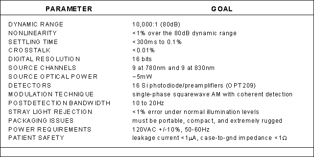
A summary of our performance goals for the prototype DOT imager is shown in the following table.
Since we planned to perform some measurements in a clinical setting, the unit had to operate within a normal hospital environment. This placed a severe stray-light rejection requirement on our design. We needed to detect picowatts of source signal under an ambient optical background in the microwatt range (as seen by the detector). We solved this problem by using synchronous detection.
Synchronous detection, is a technique which offers substantial advantages when detecting small signals buried in random, uncorrelated noise (with respect to the modulation frequency). In order for coherent detection to work, the source must be intensity-modulated in some known fashion, usually in the form of a 50% duty cycle squarewave or sinusoidal waveform, which we create by modulating the bias current through the laser diode sources.
Each photodetector preamp output is first highpass filtered to remove low frequency signals from stable interference sources like sunlight and 1/f (flicker) noise generated by the electronics. The medium frequency components produced by fluorescent lamps at 120Hz and its harmonics are somewhat attenuated as well. This filtered preamp output is then fed into a double-balanced mixer. The mixer, which is gated by the same modulator that controls the laser diode source intensity, synchronously rectifies the weak modulated source signal, which appears as a small DC voltage at the mixer output. All other spurious modulated optical signals (including those produced by line-powered lamps, computer terminals, multiplexed LED displays, etc.) which are not phase-coherent to the source will exit the mixer in the form of frequency-shifted AC signals.
A lowpass filter placed at the output of the mixer strongly attenuates these incoherent signals, leaving only the small DC voltage proportional to the magnitude of the source energy detected. The time constant of this lowpass filter controls the post-detection bandwidth, which significantly reduces the noise level, but also limits the rate at which the desired signal intensity changes can be detected. It is important to set this bandwidth as low as practical to minimize noise, since the noise is proportional to the square root of the post-detection bandwidth.
The modulation frequency, which is typically between 100Hz and 100kHz, can be adjusted slightly to shift the detection passband away from narrowband interference sources that happen to fall near harmonics of the modulation frequency. These interference sources can sometimes generate intermodulation products (undesired signals created in the demodulation process, equal in frequency to the difference between the interference frequency and the modulation frequency or one of its harmonics) within the postdetection bandwidth, which are sometimes difficult to remove otherwise.
We used a nominal modulation of 2kHz, which was chosen to shift the detection band out to a frequency region where the flicker noise was low, yet to where the detector/preamps were still capable of responding to the third harmonic at 6kHz. Although third harmonic response was not critical for operation, it served to improve the “average-to-peak” voltage ratio of the received signal, and so provided a little more dynamic range at the high end. The post-detection time constant was set at 40ms, and a dwell time of ~200ms was chosen to provide sufficient settling for each detector channel. This time constant was chosen to both provide significant noise reduction and yet remain fast enough to perform basic functional imaging studies.
Both source and detector selection was under direct, real-time computer control. This both simplified the digital design and offered us the flexibility to operate as few or as many sources and detectors as were needed. A photo of the prototype imager in operation and a functional block diagram are shown below.
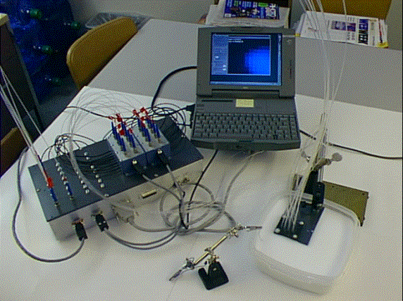
A photo showing CW1 in operation. The optode assembly is immersed in a fluid scattering phantom with a ~1cm absorber suspended in the fluid by means of a thin wire supported by the alligator clipstand. The DOT image of the absorber is visible on the computer display, which correctly reveals its location at the lower right edge of the optode array.
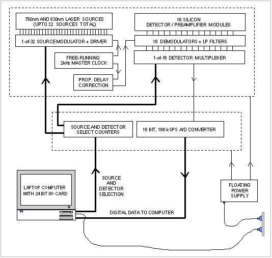
A block diagram of the CW1 prototype DOT imager, which contains nine 780nm sources and nine 830nm sources. The analog outputs of all 16 detector channels, each consisting of an OPT209 detector followed by a synchronous demodulator, are digitized on-board and then read directly to computer memory using a commercial PCMCIA data acquisition card. All functions, including source and detector selection, were computer-controlled.
The following papers report on studies using the CW1 system.
(return to the continuous-wave DOT instrument home page)